Background
A Germanium-Tin (GeSn) quantum well sandwiched between pure Germanium has recently emerged as a promising platform for engineered quantum devices. Material characterization through structural and electronic analysis displays excellent quality and performance, suitable for the full scope of electronic quantum devices based on local gates 1.
A novel research and engineering avenue would be opened up if superconductivity can be induced in the GeSn quantum well. To this end, a very transparent interface between a superconductor and the quantum well needs to be achieve, so that the superconducting correlations between charge carriers are retained upon their transfer from the superconductor into the semiconductor. Achieving this so-called ‘proximity-induced superconductivity’ would be a next major milestone for the platform, opening the full suite of hybrid superconductor-semiconductor devices.
This MSc thesis will focus on establishing a superconducting contact to GeSn quantum wells. Verification of the existence of proximity-induced superconductivity will be through observation of the Josephson effect in a superconductor - gate-tunable GeSn quantum well – superconductor device, a so-called Josephson field-effect transistor, or JoFET 2.
Your Task
The main task is to create and test a superconducting contact, using the state-of-the-art nanofabrication tools in the Helmholtz Nano Facility of FZ Jülich, and the cryogenic electronic measurement facilities in our cryolabs at the Peter Grünberg Institute of FZ Jülich. GeSn materials will be provided by the team of Dr. Dan Bucca. We envision trialing diffusion based superconducting contacts (e.g. realize creation of superconducting Platinum-Germanide PtGe2), as well as using reactive ion etching to etch down to the quantum well and seek contact with established superconductors such as Aluminum, Titanium, Niobium Titanium Nitride.
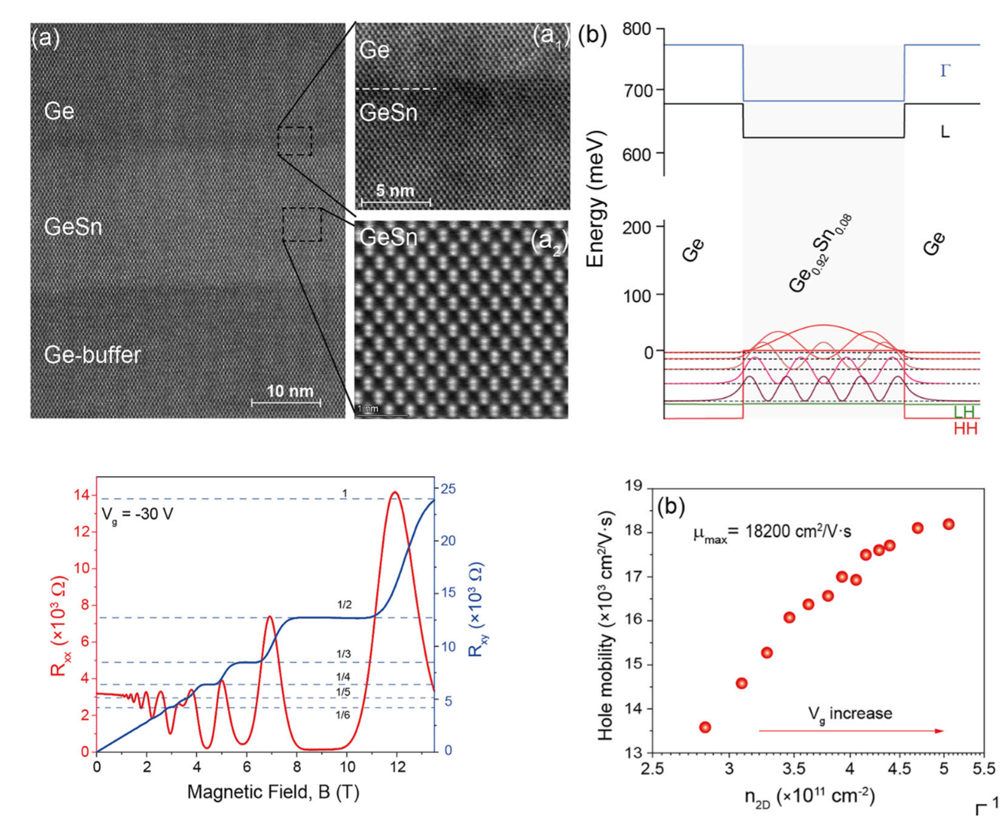 The GeSn quantum well. Top row: structural analysis through TEM imaging (left), and band structure diagram (right). Bottom row: electronic characterization with quantum hall effect (left) and hole mobility (right). Figures adapted from Fig. 1 and Fig. 2 in Ref. 1.
What we offer
- Workplace, laptop for duration of the project.
- An equivalent student assistant contract via Forschungszentrum Jülich
- Exposure to leading research activities in quantum technology
Supervision
- Dr. Vincent Mourik, FZ Jülich, PGI-11 [email protected]
- Core expertise: Josephson junction characterization, Ge-based nanofabrication
- Prof. Dr. Thomas Schäpers, FZ Jülich, PGI-9 [email protected]
- Core expertise: Josephson junction characterization, nanofabrication
- Dr. Dan Buca, FZ Jülich, PGI-9, [email protected]
- Core expertise: GeSn heterostructure development, material characterization
References
-
P. Kaul et al., GeSn quantum wells as a platform for spin-resolved hole transport, Communications Materials 6, 216, 2025. https://doi.org/10.1038/s43246-025-00934-9 ↩
-
Y-J. Doh et al., Tunable Supercurrent Through Semiconductor Nanowires, Science 309, 5732, 2005. https://doi.org/10.1126/science.1113523 ↩